![]() WIP WIP WIP WIP WIP
WIP WIP WIP WIP WIP ![]()
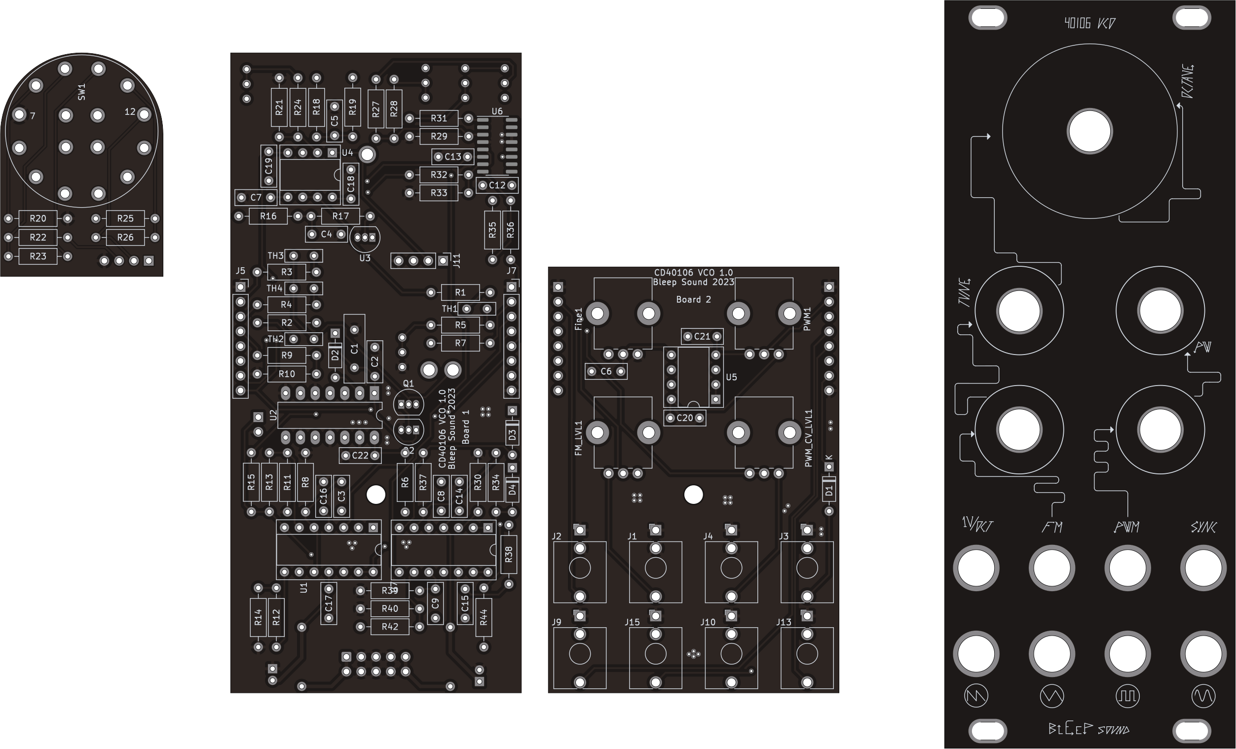
Saw-core VCO based on Moritz Klein version, with additionnal wave shaping capabilities.
Saw, Square, Sine and triangle wave output.
V/Oct, PWM and FM CV inputs.
Hard Sync input.
Octave switch and pot for fine control for each octave.
Octave switch and additionnal wave shapping taken fron Ray Wilson on MFOS
Extension connector (back of board) to connect to the SubPhatty extender (Sub octave extender, WIP).
Module Specs
Eurorack standard, 3U 10HP
| rail | Power |
|---|---|
| +12V | 37mA |
| -12V | 31mA |
| 5V | 0mA |
Schematics


BoM
You can donwload the bom in excel format here
Build Informations
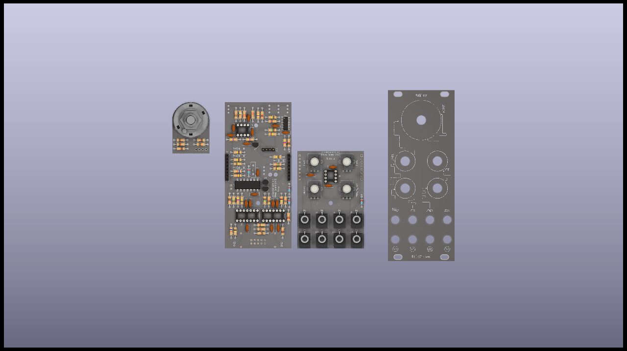
Uses an SMD LM13700 because the DIP ones are not produced anymore.
Regular build, I use ceramic capacitors but you can use film/polyester.
Polyester capacitor for the saw core.
![]() When building modules, always do it in this order (from smallest component to highest):
When building modules, always do it in this order (from smallest component to highest):
- diodes
- resistors
- DIP chips
- capacitors (film/ceramic)
- Transistors
- Electrolytic capacitors
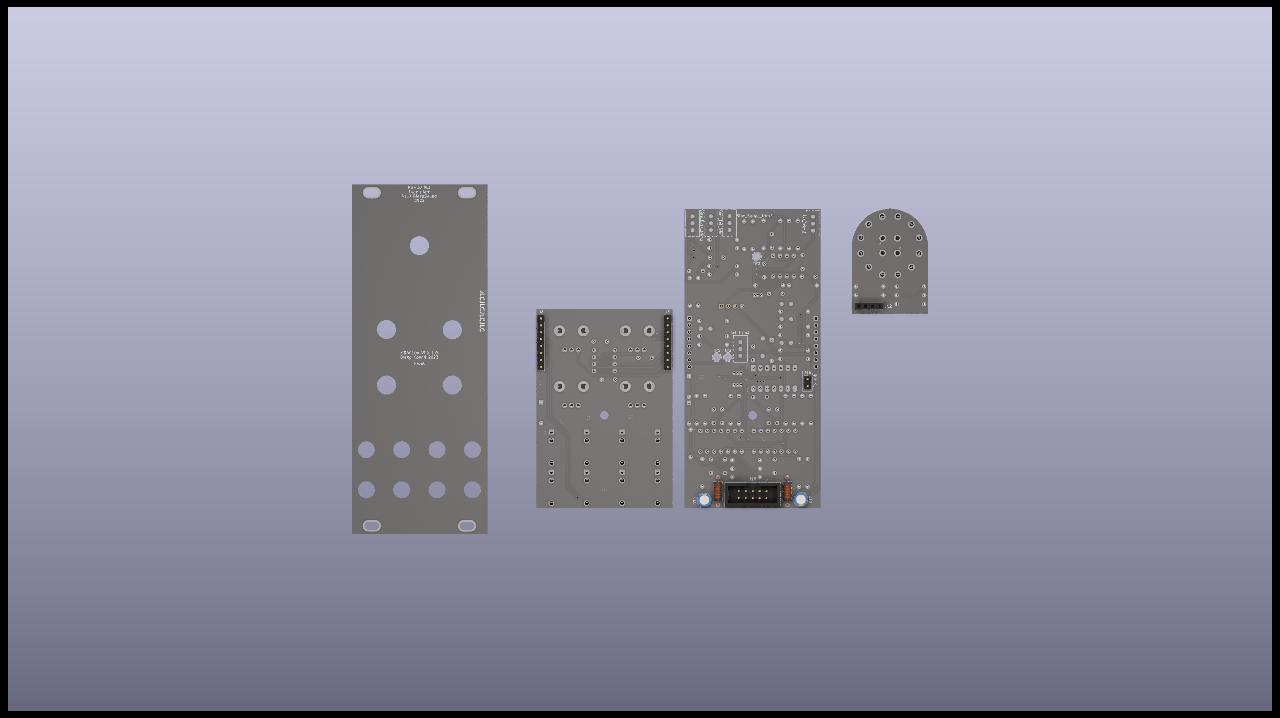
To solder the headers, place them and place both PCBs in their final position before fully soldering the pin headers/sockets.
For the next parts, always place them without soldering them on:
- jacks, pots and switches that go throught the front panel
Once placed, put the front panel in place, then fasten all components to it. Once this is done, you can solder all the remaining components.
For the rotary switch, you have pin markings on it. make them correspond to the pin marking on the PCB, then you can solder it.
To connect the switch board to the main PCB, use wires and follow the marking on both PCBs.
Calibration
5V reference voltage
This module uses a 5V voltage reference for the octave switch. To make sure we have the proper reference, you need to make sure we have a proper 5.00V setup internaly. Use a multimeter at Test point 3 and use the trimmer lvl_Trim2 to read exactly 5.00V here.
Sin wave approximation
To get the Sin wave out of this VCO, a litle something called non-linear distortion is done to the triangle wave. You have 3 trimmers on the back of the module to setup that distortion properly.
You are going to need an oscilloscope and your ears. Plug your oscilloscope to the sine output of the VCO. Refer to the below figures to setup the best possible sine wave for the VCO.
Sine_bias_trim1, adjust for top to bottom symmetry and for least sine distortion.
Sine_Shape_Trim1, adjust between too square and too triangle.
Sine_Levl_Trim1, adjust for +/-5V
Tuning
And the final step, tuning the VCO, you are going to need a digital tuner (or your ears if you have perfect pitch!).
Set your octave switch to low C (0V) and move your fine pot so you get a low C on your tuner.
Once done, set your octave switch to high C (5V), and you want to hear a high C here, but usually, you will get something that’s completely off the mark. Use the trimmer lvl_Trim1 to get to a high C. This is trail & error, so it might take you a few tries.
And that’s it, the VCO is now fully calibratedr and tuned !
Images
Version
V1.0
Do Not Use
- First prototype, loads of issues, ranging from wrong value resistors, to wrong orientation on transistors.
- Wrong hole size on front panel for octave switch
V2.0
- Fix issues identified on v1.0
- Update front panel
- Add calibration info to website
Download
Follow this link if you want to dowload the latest version of gerber files, schematic, kicad files…
![]()
This work is licensed under a Creative Commons Attribution-ShareAlike 4.0 International License.

Leave a comment